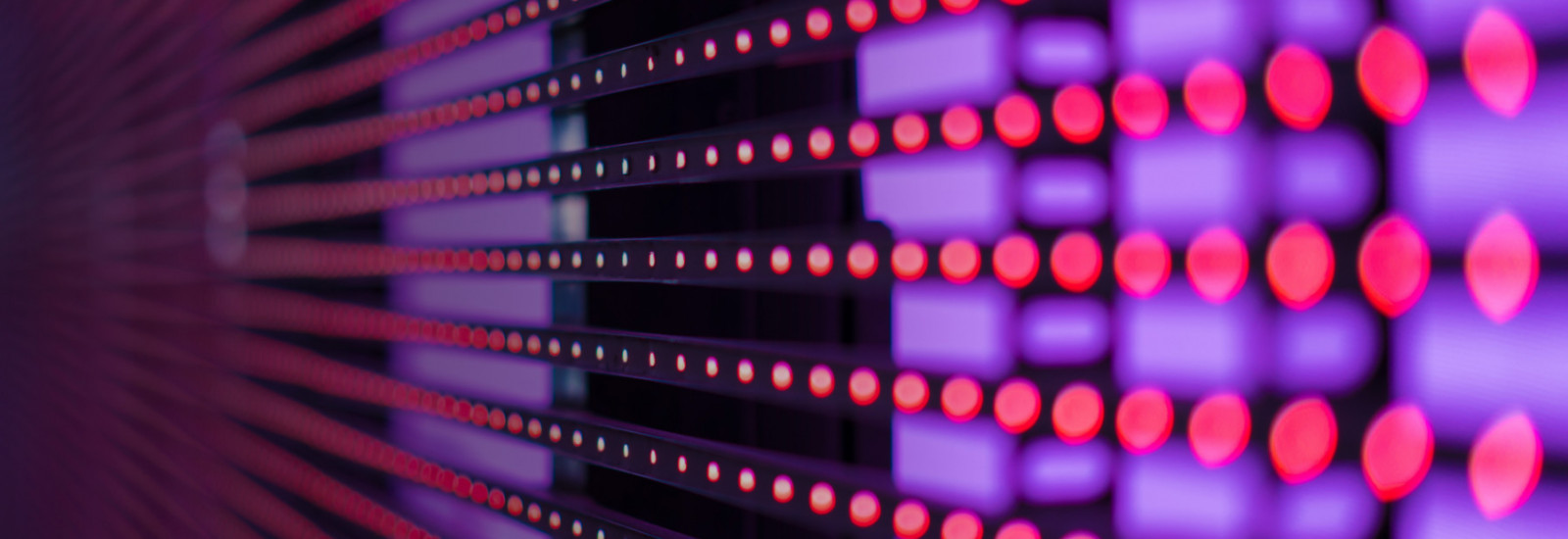
Liquid crystal displays (LCDs) are an indispensable component of modern televisions, smartphones and tablets. In an LCD screen, light-emitting diodes (LEDs) generate white background light, which then shines through an ultrathin liquid crystal layer toward the viewer. The crystal layer is divided into numerous segments (pixels) whose respective light transmission can be regulated by applying an electric field. In this way, each pixel shines with its own unique brightness (and color via color filters).
In flat-panel TVs with conventional LEDs, the necessary backlighting is generated by a few hundred LEDs; more than that is not possible due to the comparatively large space required by the individual LEDs. The disadvantage is obvious: A truly homogeneous illumination of the LCD screen is not possible with such a coarse LED matrix. Accordingly, there was great enthusiasm in the industry when the first screens with the novel mini-LED technology came onto the market in 2020. Since mini-LEDs are extremely small (0.05 to 0.2 mm) compared to classic LEDs, the backlight can now be generated from tens of thousands of mini-LED light sources. The mini-LEDs are bundled into so-called illumination zones, whereby each zone is still significantly smaller than a conventional LED. By controlling the individual zones in a targeted manner, the intensity of the backlighting can be spatially controlled much better than was the case with conventional LEDs. As a result, the TV viewer can look forward to significantly improved contrast and a deeper black. In addition, mini-LED technology excels at producing an exceptionally high dynamic range (HDR) and also consumes less power.
The basis of it all: Light-emitting diodes
The manufacture of LEDs or mini-LEDs is far more complex than the apparent simplicity the component suggests – not least because some essential manufacturing steps have to take place under vacuum conditions. In the first step, a wafer is coated with a metal-organic layer using the MOCVD (metal organic chemical vapor phase deposition) process. In this process, the layer substance attaches itself to the existing crystal lattice in an atomically ordered manner: The layer, which is only a few atomic layers thick, exactly adopts the crystal structure of the wafer. To ensure that the coating does not contain any impurities, this process step must take place under the protection of a vacuum. This is where valves from VAT come into play. The world's largest manufacturers of MOCVD systems – with company headquarters in Germany, China and the USA – rely on VAT vacuum valves.
To create the positive-negative transitions in the LED, additional ultrathin layers must be deposited and then etched away in the right places. This delicate task is best accomplished through an interplay of two plasma-enhanced thin-film processes: Plasma-enhanced chemical vapor deposition (PECVD) is used to deposit the layers, and plasma chemical dry etching is used to partially remove them. Since these processes must also be carried out under vacuum conditions, VAT vacuum valves play an important role here as well.
The VAT valve portfolio for MOCVD, PECVD and dry etch applications includes:
- Transfer valves for transferring the substrate into and out of the individual vacuum chambers (load-lock, transfer and process chambers). Tailored to customer requirements as inserts, installed directly in the chamber or installed classically with flange-mounted housing (e.g. series 02.4 with MONOVAT technology or 04.2 or 07.8 each with L-VAT technology).
- Control valves for pressure control in the vacuum chamber as Butterfly Valve (e.g., series 61.3) or as Pendulum Valve (e.g., series 65.3)
- Isolation valves for separating vacuum pumps or pump lines from the chambers, as gate valves (e.g., series 12.1) or angle valves with soft-pump function (e.g., series 29.0)
Paradigm shift thanks to micro-LEDs
VAT valves will certainly also be part of the party in the future when the actual breakthrough comes. After all, according to experts, mini-LEDs are just a stopover on the way to even smaller light sources: micro-LEDs. These truly microscopic components are smaller by a factor of 50 to 100 compared to mini-LEDs. Be amazed: The edge length of the smallest micro-LED is currently 3 micrometers, or three-thousandths of a millimeter! But it is not only the difference in size that makes micro-LEDs so special. Rather, micro-LED technology represents a real paradigm shift. In contrast to LCD screens, where (mini) LEDs play a rather inconspicuous secondary role as a background light source, in micro-LED screens every single pixel is self-luminous, dimmable and can be switched off completely. Additional backlighting – and the associated technical uncertainties – is therefore no longer necessary at all!
As small as the micro-LED is, its effect is huge. The transition from mini- to micro-LED technology brings weighty advantages. Some of them are visible, such as the larger color spectrum, higher brightness, sharper contrast and faster refresh rates. Others, such as lower power consumption and longer life, are intangible but no less significant. Against this background, it is highly likely that this new generation of LEDs will become a veritable game-changer.
